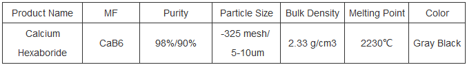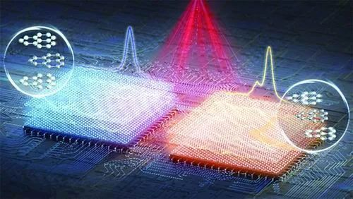
Press reporters from China discovered on the 14th that scientific researchers from the Institute of Physics of the Chinese Academy of Sciences, the National Nanoscience Center, and various other devices, with examining the rhombic stacking structure of three-layer graphene, located that in the rhombic stacking of three-layer graphene, electrons, and Infrared phonons have solid communications, which are expected to be utilized in areas such as optoelectronic modulators and optoelectronic chips. Pertinent research outcomes were released online in the journal “Nature-Communications”.

(graphene solutions)
Schematic illustration of stacking-related electroacoustic combining in three-layer graphene. The left is a three-layer graphene stack of ABA; the right is a three-layer graphene pile of ABC. (Picture courtesy of the research group)
In recent times, three-layer graphene has actually brought in extensive focus from researchers. Generally, three-layer graphene can exhibit 2 different stacking geometric configurations, namely rhombus piling and Bernal stacking. “These 2 kinds of stacked three-layer graphene have totally various proportions and electronic buildings. As an example, the centrally balanced rhombus-shaped piled three-layer graphene has a power gap flexible by a displacement electrical area and can exhibit a collection of Bernal Piling three layers of graphene does not have appropriate physical impacts: Mott insulating state, superconductivity and ferromagnetism, etc,” stated Zhang Guangyu, co-corresponding author of the paper and scientist at the Institute of Physics, Chinese Academy of Sciences.
How to recognize these uniquely related physical effects in three-layer graphene rhombic stacks has actually turned into one of the current essential research frontiers. This time around, the scientists uncovered the strong interaction between electrons and infrared phonons in rhombic piled three-layer graphene through Raman spectroscopy with flexible gateway voltage and excitation frequency-dependent near-field infrared spectroscopy. “We suggested a basic, non-destructive, high spatial resolution near-field optical imaging innovation that can not only recognize the stacking order of graphene however additionally discover the solid electron-phononon communication, which will certainly provide leads for multi-layer graphene and edge. It gives a strong foundation for research on graphene,” said Dai Qing, co-corresponding writer of the paper and researcher at the National Facility for Nanoscience and Modern Technology of China.
This research gives a new perspective for recognizing physical results such as superconductivity and ferromagnetism in three-layer graphene piled in a rhombus. At the exact same time, it also provides a basis for related material study for the layout of a brand-new generation of optoelectronic modulators and chips.
High Purity Nano Graphene Supplier
Graphite-crop corporate HQ, founded on October 17, 2008, is a high-tech enterprise committed to the research and development, production, processing, sales and technical services of lithium ion battery anode materials. After more than 10 years of development, the company has gradually developed into a diversified product structure with natural graphite, artificial graphite, composite graphite, intermediate phase and other negative materials (silicon carbon materials, etc.). The products are widely used in high-end lithium ion digital, power and energy storage batteries.If you are looking for single layer graphene, click on the needed products and send us an inquiry: sales@graphite-corp.com
Inquiry us